
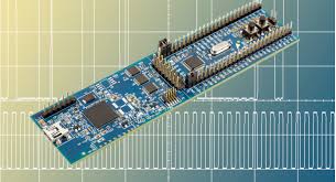
The process of fabricating printed circuit boards (PCBs) needs complex procedures to guarantee the top performance of the finished product. Circuit boards come in double, single, or multilayer boards, and the PCB fabrication process will only differ once the first production layer is done. The difference in the structure of PCBs results in some needing up to twenty steps during manufacture. The complexity of PCBs correlates to the number of procedures required to manufacture the boards. These steps are critical, and skipping one or cutting back on the steps can result in poor-performing circuit boards. However, when the process of PCB fabrication is done according to set guidelines, the circuit boards will work perfectly as essential electronic components.
The Steps of PCB Fabrication
The steps involved in PCB fabrication are critical and must be followed religiously to guarantee quality circuit boards. The steps are many, depending on the number of layers incorporated. These steps include: Designing the PCB; Design Review and Engineering Questions; Printing the PCB Design; Printing the Copper for the Interior Layer; Etching the Inner Core to Remove Copper; Layer Alignment; Automated Optical Inspection; Laminating the PCB Layers; Drilling; PCB Plating; Outer Layer Imaging; Outer Layer Etching; Outer Layer AOI; Solder Mask Application; Silkscreen Application; Finishing the PCB; Electrical Reliability Test; Profiling and Route Out; Quality Check and Visual Inspection; and Packaging and Delivery. As stated earlier, no step should be skipped when manufacturing PCBs.
Parts of Printed Circuit Boards
Printed circuit boards have four major parts. These are highlighted below.
Substrate
The substrate is one of the essential parts of printed circuit boards. It is made of fiberglass. Fiberglass is used to make the substrate because it offers the core strength needed by the PCB. This helps to resist any breakage of the final product. The substrate is the skeleton of the printed circuit board.
Copper Layer
The copper layer is another critical element of the printed circuit board. Depending on the type of board, the copper layer can be a full copper coating or a copper foil. This layer is responsible for carrying electrical signals to and from the printed circuit board. Copper is a good electricity transmitter, making it the ideal choice for this layer.
Solder Mask
The solder mask is the third piece of the printed circuit board. This is a polymer layer that is laid down during PCB fabrication to act as a protective layer. It protects the copper layer, preventing it from short-circuiting due to coming into contact with the immediate environment. This serves as the ‘skin’ of the printed circuit board.
Silkscreen
The silkscreen is the fourth part of the printed circuit board. This is located on the component section of the circuit board that displays part numbers, component references, logos, test points, and symbol switch settings.
Conclusion
The PCB fabrication process is delicate as it involves several steps that have to be followed precisely. However, none of the fabrication steps have to be skipped or cut back to guarantee a top-performing printed circuit board. In addition, the components found on the PCB ought to be handled with care and installed correctly.